ALL Products
-
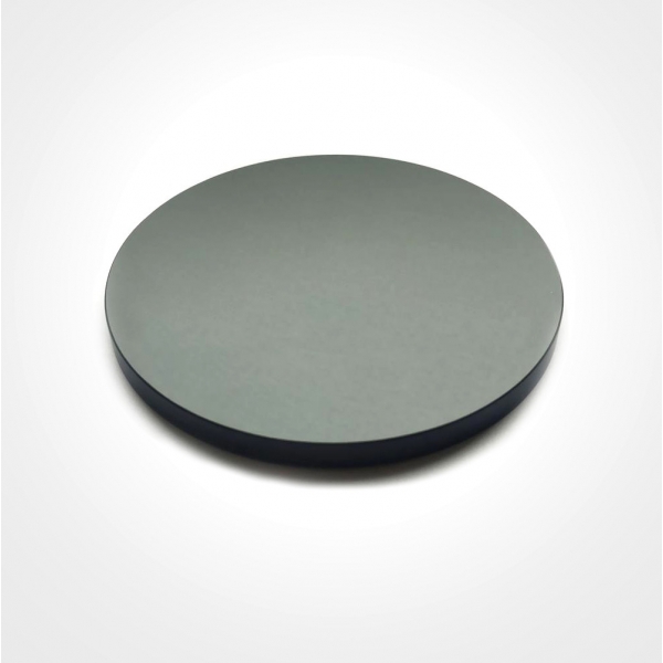
 Optical coatingOptical coatings are deposited as thin-films of a variety of materials.
DETAILOptical coating -
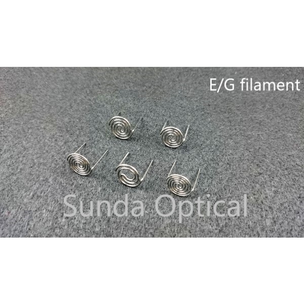
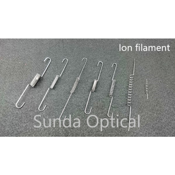
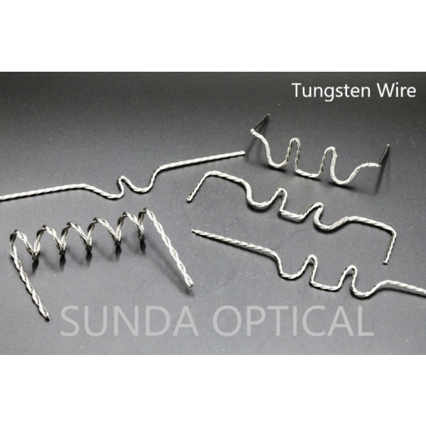 Tungsten coilsTungsten filaments in a variety of shapes and numbers of wires.DETAILTungsten coils
 -
 Transparent conductive filmIt is the key material that have been widely used in industries in recent years.DETAILTransparent conductive film
 -
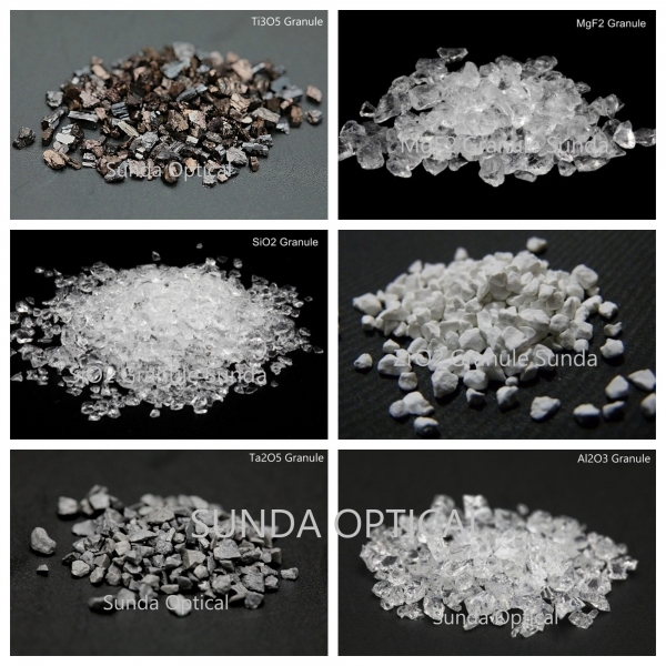
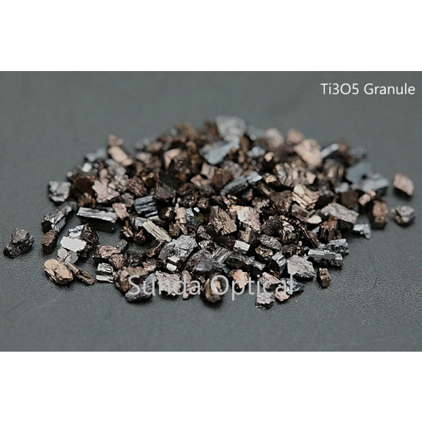 Evaporation material-Ti3O5The common types are granules and tablets.DETAILEvaporation material-Ti3O5
 -
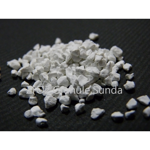 Evaporation material-ZrO2The common types are granules and tablets.DETAILEvaporation material-ZrO2
 -
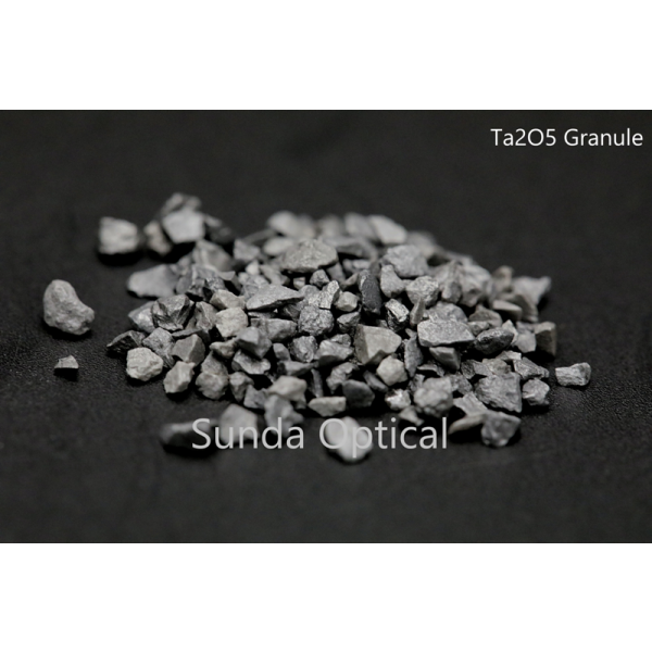 Evaporation material-Ta2O5The common types are granules and target.DETAILEvaporation material-Ta2O5
 -
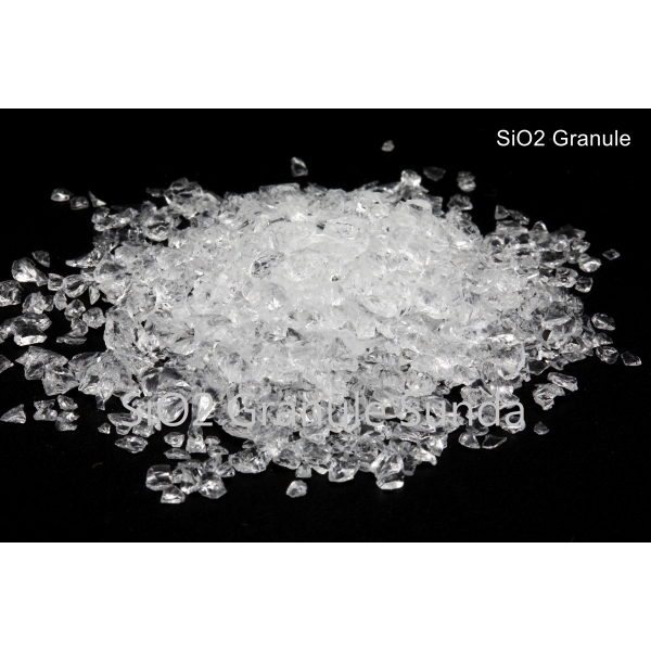 Evaporation material-SiO2、SiO2 ringThe common types are granules and tablets.DETAILEvaporation material-SiO2、SiO2 ring