


Sputtering target is a material which commonly used in the semiconductor and optoelectronic industries.
The sputtering process begins when a substrate to be coated is placed in a vacuum chamber containing an inert gas - usually Argon - and a negative charge is applied to a target source material that will be deposited onto the substrate causing the plasma to glow.
Free electrons flow from the negatively charged target source material in the plasma environment, colliding with the outer electronic shell of the Argon gas atoms driving these electrons off due to their like charge. The inert gas atoms become positively charged ions attracted to the negatively charged target material at a very high velocity that “Sputters off” atomic particles from the target source material due to the momentum of the collisions. These particles cross the vacuum deposition chamber of the sputter coater and are deposited as a thin film of material on the surface of the substrate.
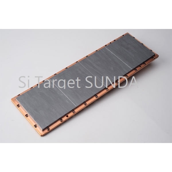
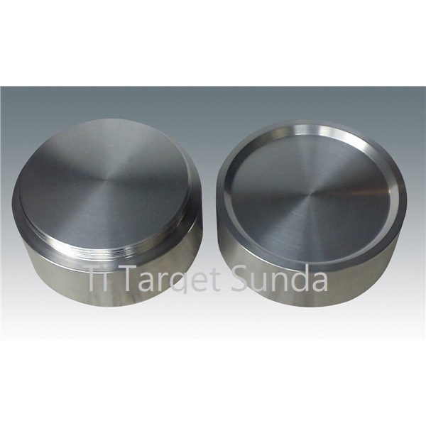
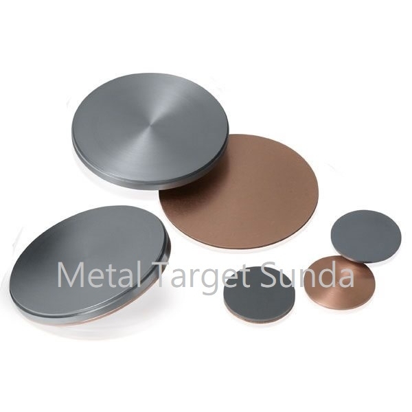
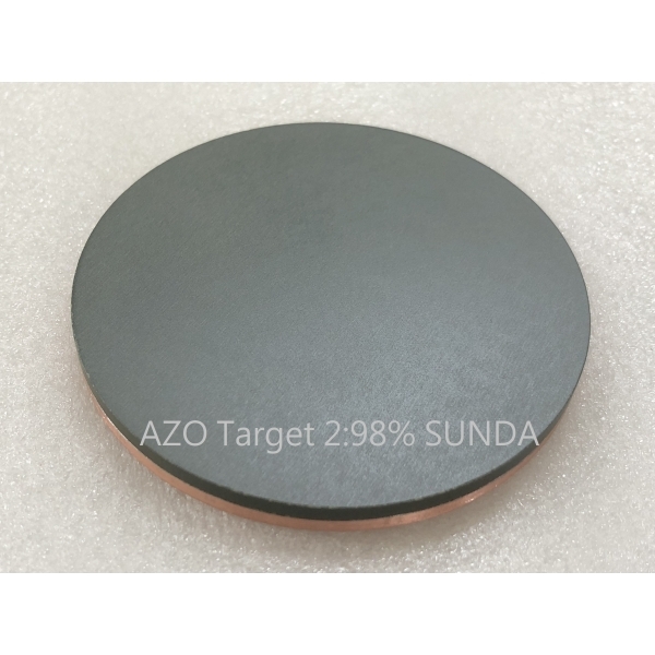
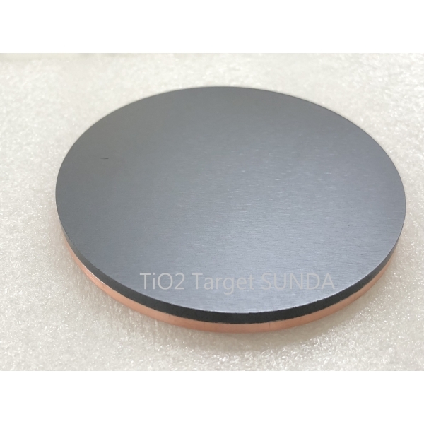
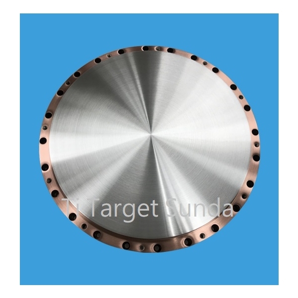
Sputtering targets are typically high purity compound, or pure metals, requiring a purity of at least 99.99%. Their shape looks like a thick disc, and some are long strips, depending on the specifications of the sputtering equipment.
Since pure metal targets have thermal conductivity themselves, they don’t need to be bonded. On the other hand, compound targets do not have thermal conductivity; they need to be bonded with a copper plate in order to conduct heat.
.jpg)
Sunda Optical Material provides bonding services depending on the target of different materials, and the specifications can also be customized according to your requirements. In addition to the bonding service, we also provide metal detection service before targets leave the factory.
During the coating process, there are target fall off conditions due to human or material factors. For this part, please refer to FAQ on our website, or leave us a message. We’re willing to help you!